

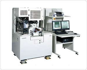
집속이온빔장치1 (FIB1)
| 사진 |
 |
|---|---|
| 영문명/단축명 | Focused Ion Beam 1 / FIB1 |
| 모델명 |
SMI 3050TB |
| 설치장소 | 미세구조분석실 / [81B104]집속이온빔(FIB) |
| 제작사 | SII |
| 도입년도/가격 | 2006.3월 / 705,000,000원 |
| 담당자 / 연락처 / e-mail | 정효인(Jung Hyoin) / 031-299-6777 / hyoin@skku.edu |
♦ Features
• The ion beam optical system attains an image resolution of 4 nm or less and a maximum current density of 30 A/cm2 or greater, enabling observation using clear, high-resolution imaging
• The system dramatically improves performance at the low ion beam acceleration voltage setting (5kV), facilitating high-precision processing with sample damage minimized at low acceleration, which has been difficult to achieve in the past. In addition, with the improvement of ion beam performance with ion currents in the minimum subpicoampere range, processing at the nano meter order is now easily achieved
• The electron beam optical system enables use of the FIB-SEM hybrid system for microscopic observations of the area processed with FIB at a resolution of 5 nm or less (acceleration voltage:1 kV), which is the resolution of the world’s highest standard. In addition, the system also realizes real-time monitoring of FIB processing by simultaneous electron beam irradiation
• Inclining the electron beam optical system against a vertically positioned ion beam optical system permits SEM observation of the cross-section of the sample exposed by FIB sputter etching without requiring inclination of the sample
• The sample fabrication software used for TEM observation, improves the throughput and processing precision that come with improvements in FIB performance
• Use of state-of-the-art pattern recognition technology greatly reduces the necessary setup work prior to processing
♦ Specification
• Triple Beam System(SEM, FIB, Ar Ion Beam)
• FIB Processing observed in real time by SEM
• Maximum Probe Current Density : Bigger than 30A/cm2
• Maximum Probe Current : 20nA