

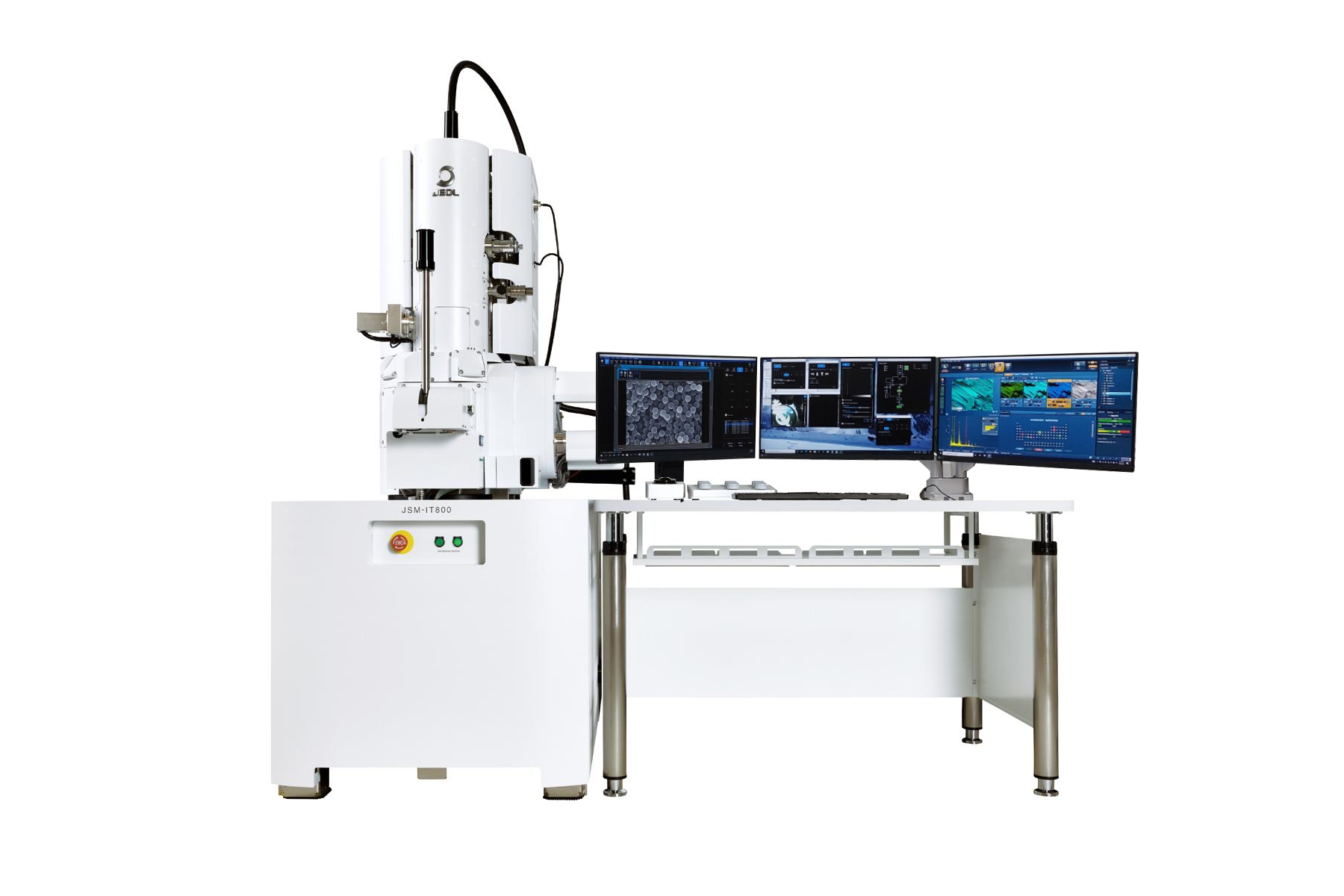
초고분해능전계방사주사전자현미경5(SEM5)
| 사진 |
 |
|---|---|
| 영문명/단축명 | Field Emission Scanning Electron Microscope 5 (EDS/EBSD)/FESEM 5 (EDS/EBSD) |
| 모델명 | JSM-IT800 |
| 설치장소 | 미세구조분석실//[81B106]주사전자현미경실 |
| 제작사 | JEOL |
| 도입년도/가격 | 2021년 2월/826,945,095원 |
| 담당자/연락처/e-mail | 조현진(Cho Hyunjin) / 031-299-6749 / hjjo@skku.edu |
♦ Features
• JSM-IT800 accommodates four detectors(UED, UHD, BED, SED)
• Selecting observation conditions and detectors suitable for your applications enables you to acquire characteristics SEM Images (compositional, topographic, morphological, crystalline information)
• In-lens Schottky Plus FEG generates electrons can be efficiently and also provides high resolution images at low accelerating voltage
• SEM Images with high S/N at low accelerating voltage
• When using the UHD mode to detect the signals, can reduce the charging effects
• It is suitable for observing the non-conductive specimen with nano-structure and easily damaged by electron beam(minimize sample damage)
• Single nm steps are clearly observed on the particle surface
♦ Additional Options
• EDS Detector: ULTIM MAX 170
- High spatial resolution and speed within several minutes by 170 mm2 Area detector (Quantitative analysis at >400,000 cps , Mapping at >1,000,000 cps)
- Minimise sample damage
- Minimise sample contamination
- Provide more detailed analysis
• EDS Detector: ULTIM EXTREAM(windowless type EDS)
- The Ultim Extreme is a windowless 100 mm2 and maximise sensitivity and spatial resolution
- Fantastic sensitivity to light elements such as nitrogen
- Low kV analysis reducing/eliminating sample damage and charging
- Fast data collection with higher count rates compared to traditional detectors
• IT-800 EBSD
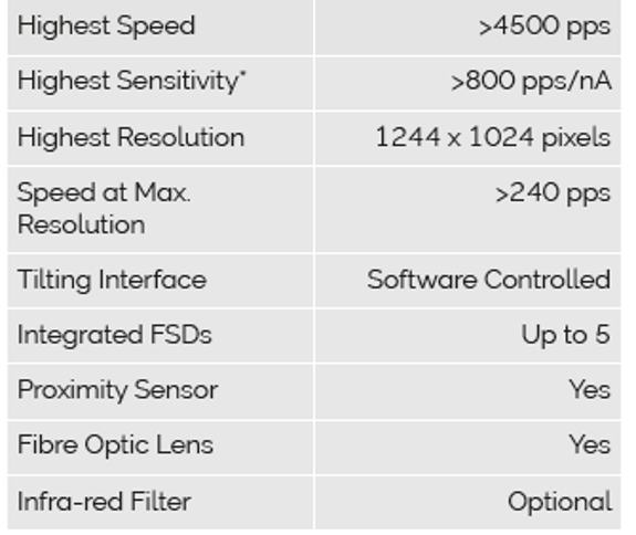
- Symmetry S2’s fibre optics deliver 2-3 times better sensitivity than standard detector
* Symmetry S2: 3100pps(39min)
* Standard: 1350pps(1.5hrs)
- High quality and faster diffraction patterns enable effective materials characterization in a short time
- Re-analysis is possible by required EBSD pattern
- From EBSD we obtain?
* Grain size, Grain boundary characterisation, Phase distribution, Texture(or crystallographic preferred orientation), Orientation data, Strain and deformation
♦ Specification
• Resolution: 0.7nm(20kV), 1.3nm(1kV), 3.0nm(15kV, 5nA, WD10mm)
• Magnification: x10 to x2,000,000(128 x 96mm)
• Acc. Voltage: 0.01 ~ 30kV
• probe current
- A few pA to 300nA(30kV)
- A few pA to 100nA(5kV)
• Detector(Standard)
- SED(Secondary electron detector)
- UED(Upper electron detector)
• Electron gun: In-lens Schottky Plus