


Nano Devices
Our research focuses on nano-electronics having strong potential and high impact for future application in the areas of DNA based molecular-electronics, high-k based non-volatile memories, quantum electronics, and photonics.
Particular Research
-
Nano- and Bio-electronics & Fabrication
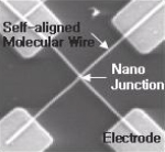
- The method of transforming DNA into molecule semiconducting wire
- The nanowires using the conjugation of DNA and metal
- The new technique to form the Nanometer scale gap in metal electrode
-
MRAM, FRAM, SCM, Molecular Devices
- Characterize a electrical and a physical properties of MTJ cells using SPM.
- Polarization properties of ferroelectric thin film are characterized with KFM and SNDM.
- Analyze the doping concentration and profile of nano-scale electric device, using the SCM
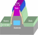
- Making 3 terminal devices of molecular electronics
-
High-K Dielectric Materials and Etching
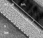
- High-k HfO2 and ZrO2 for flash memory application
- Dual Charge Storage Layer
- Deep via etching
-
Fundamental Physics, III-V Mlecular Beam Epitaxy
- Low dimensional electron transport, multilayer two-dimensional electron systems, quantum computing using surface acoustic wavers and single photon detector
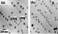
- High mobility modulation-doped 2D electron gases, quantum devices fabrication by growth, self-assembled quantum dots and magnetic thin film and spin injection devices
- Transport through single molecules-molecular electronics and selective self- assembly and molecular recognition with DNA
-
Nano-photonics & Semiconductor-based Photonic Device
- Ultrasmall photonic chips, trapping of photons, single photons source for quantum communication, bio-chemical sensor, nonlinear optical devices, and so on.